Last Modified: 30 September 2012
Thermionic Valves
Theory of Operation, Types, and Basic Amplifier Circuits
Index
Valves:
- Electron Emission
- The Thermionic Diode
- The Triode
- Triode Characteristics – Deducing
- The Tetrode
- The Pentode
- Beam Tetrodes
- The Variable-mu Pentode
- Basic Valve Circuits
Transformers:
- Making Valve Mains Transformers
- Valve Rectifiers for Mains Transformers
- Making High Inductance Chokes for HT Smoothing 'pi' Filters
- Making Single-Ended Audio Output Transformers
- Making Push-Pull Audio Output Transformers
Appendix:
- Sources:
- 1. Electronic Systems and Technology by K.F. Ibrahim 1878, 1981
- 2. not sure, an American book but I only have photocopies, probably by RCA
- 3. Coil Design and Construction Manual by B.B. Babani 1960 – 1989
Copyright © Maplin Electronics plc 1993 and Graham Dixey
Part 1 – Thermionic Emission and Valves
Electron Emission
A conductor contains a large number of free or loose electrons. These electrons may leave the surface of the conductor if given enough energy to overcome their attraction to their nuclei. Such energy may be provided by heat, electron bombardment, or light. The emitting conductor is always placed in a vacuum to facilitate the emission.
- Thermionic emission which occurs when a conductor is heated. If sufficient energy is given to the electrons, they leave the surface. This type is sometimes known as primary emission.
- Secondary emission which occurs when high-velocity electrons strike a conductor in a vacuum, knocking out one or more electrons from the surface.
- Photo-emission occurring when energy in the form of light falls upon the surface, knocking out electrons.
The Thermionic Diode
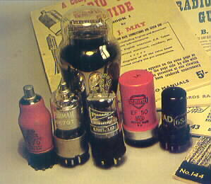
An electrode known as the cathode is placed inside an evacuated, sealed glass bulb, called the 'envelope'. (For convenience and economy of space, in practice it is common for two or more separate thermionic devices to share one envelope.) The method of construction is very much like that for a light bulb, and is no coincidence – the thermionic valve directly followed and is descended from the development of the electric light bulb.

Figure 01
The cathode may be heated directly by passing current through it, or indirectly by an insulated heating filament inside (see Figure 01  ). In the latter case the cathode is a metal tube. Electrons thus begin to be emitted from the surface into the vicinity of the cathode, filling the space around it with negatively charged electrons. (To improve efficiency, the outside of a real cathode is further coated in a compound that most readily emits electrons when heated.) A space charge is then said to exist in the vicinity of the cathode. As emission continues, the negative space charge begins to repel the emitted electrons, and emission ceases.
If a positive electrode known as the anode is placed facing the cathode, and a potential applied, electrons from the space charge will be attracted to it and a flow of current from cathode to anode will take place. The anode must be made positive with respect to the cathode otherwise no current flows. Hence the valve is a undirectional device known as a thermionic diode (has 2 electrodes), and this is the origin of the collective name, "valve", as in one way only.

Figure 02
The characteristics of the thermionic diode are shown in Figure 02  . From A to B the curve is similar to a semiconductor pn junction. At B the diode saturates when the anode collects all the electrons emitted by the cathode. The use of the thermionic diode is thus restricted to its linear region AB.
The circuit symbol and the basic construction of the thermionic diode are shown in Figure 03  .
.

Figure 03
To achieve higher currents requires an increased electron flow. This is only made possible by increasing the surface area of the cathode, its temperature, or both. Such high current diodes exist as the AC rectifiers for mains sourced power supplies, having very large electrode areas and high current heaters.
The Grid As A Control Electrode
The addition of a control grid to the thermionic diode by deForest in 1906 (forming the triode) made possible the control of power by an electric field in a vacuum. Later Hull and others added more grids to form the tetrode and pentode, and there were other specialised types as well.
A thermionic cathode emits electrons having an energy spectrum presented in Figure 07a. The area under the curve to the right of 0.4 eV represents electrons able to move against a –0.4 V potential; larger fractions of the total could move against –0.3 V or –0.2 V potentials. By variation of a retarding potential on an electrode facing the cathode, the number of electrons leaving the cathode can thus be controlled. This is the principle of the triode.

Figure 04
The Triode
A wire mesh known as the control grid is placed between the cathode and the anode, forming a triode (3 electrodes – Figure 04 ). The grid is placed in the space charge near the cathode. The potential of the grid thus determines the space charge density, which in turn controls the flow of electrons to the anode. Because the grid is placed close to the cathode, a small change in its potential produces a large change in anode current, hence amplification. The physical structure of such a triode is shown in Figure 07 below .

Figure 07
The anode is made positive relative to the cathode, and is attractive to electrons. A potential minimum is present near the cathode surface, due to the space charge established by the emitted electrons. If a grid of wire mesh is placed in this space-charge region, it can alter the electric field facing the electrons at the cathode surface. Being a mesh, the grid can establish this field without appreciably interfering with the electronic movement to the anode.
The potential of the grid influences the field at the cathode surface and adds to or nullifies the accelerating field due to the positive potential on the anode. With anode to cathode potential of eb, and grid to cathode potential of ec, it may be reasoned that the current passing between anode and cathode is related to these potentials as:
ib = f(ec, eb) (9-1)
The grid is closer to the cathode than is the anode, and the field produced by a one volt change on the grid is more effective in varying the current than is a one volt change on the anode. The amplification factor μ(Greek 'mu') is defined as the ratio of the effectiveness of a potential change at the grid to the same potential change at the anode. Equation 9-1 may then be modified to form the basic law of the triode:
ib = f(μec + eb) (9-2)
The grid has an appreciable area in the electron stream, but when it is negative to the cathode, few electrons will have sufficient energy to override the potential and reach the grid. Normal small-signal amplifiers are so operated and grid current is negligible (what there is being colloquially called 'grid-leak'). At positive grid potentials considerable grid current will be present; characteristics in the positive grid region may be nonlinear, and positive grid operation is permitted largely in power amplifiers.
Circuit Notation
As for the transistor, there is a standard circuit notation established by the Institute of Electrical and Electronics Engineers. Because of the early development of the triode, the notation reflects historical usage and lacks some of the network formalism common with the transistor. For instance, in the early days of radio broadcasting, the batteries supplying filament, plate (anode), and grid circuits were labelled A, B, and C; these letters have carried over as subscripts. Use is also made of g, k, and p as parameter subscripts on quantities related to the grid, cathode, and anode (plate) circuits. (Latterly however 'a' is substituted for 'p'.)
As for the transistor, lower-case letters designate instantaneous or varying currents or voltages and upper-case letters denote rms or DC values. Some of the more common symbols were:
ec = instantaneous total grid-cathode voltage
eg = instantaneous value of AC component of grid-cathode voltage
Ec = average or quiescent value of grid-cathode voltage
Eg = effective or rms value of AC component of grid-cathode voltage
ib = instantaneous total anode current
ip = instantaneous value of AC component of anode current
Ib = average or quiescent value of anode current
Ip = effective or rms value of AC component of anode current
eb = instantaneous total anode voltage
ep = instantaneous value of AC component of anode voltage
Eb = average or quiescent value of anode voltage
Ep = effective or rms value of AC component of anode voltage
Ebb = anode-circuit supply voltage
Ecc = grid-circuit supply voltage
Some valves have more than one grid and numerical subscripts are used, as ec1, ec2, With the grid nearest the cathode considered grid 1. (Latterly this is simply g1, g2, etc.)
A typical triode amplifier circuit appears in Figure 19a. The diagrams of Figure 08 illustrate the following circuit relations:
ec = Ecc + eg (9-3)
ib = Ib + ip (9-4)
Eb = Ebb – IbRL (9-5)
eb = eb = Eb – ipRL (9-6)
eo = –ipRL = eb – Eb (9-7)
The last expression points out that the output voltage is to be taken as a rise from the common terminal. Justification for the other expressions should be evident from Figure 08 .

Figure 08
Volt-Ampere Characteristics Of The Triode
Since the triode is a nonlinear circuit device, one means for expressing its operating characteristics is by families of volt-ampere curves. Since triode operation has been predicted by a functional relation of three variables, a surface is really indicated as the proper geometric relationship, but this can be represented by three sets of two-variable curves, with the third variable as a parameter in each case (Figure 09 below ).

Figure 09
Figure 09(a) relates the input voltage ec to the output current ib; these are the transfer curves. A second family in (b) relates the anode current and anode voltage; these are the output curves. The third family in (c) relates the input voltage and the output voltage required to maintain a constant current; therefore they constitute the constant-current family.
Grid Cutoff
For a given anode voltage, the transfer curves indicate that a sufficiently negative grid voltage will bring the anode current to zero, and that grid voltage is called the cutoff voltage. It may be reasoned from the definition of μ that:
cutoff ec = –(eb / μ) (9-8)
Valve Parameters
While a transistor is a current controlled current amplifier, an amplifying valve behaves more like a voltage controlled resistance. Yet, as in the case of the transistor, the valve is employed in circuits in which it is the change in current produced by a change in voltage that is of interest. The change takes place around an operating point on the curve, so that for a change of i the corresponding change in e will be found along the slope of the curve.
Triode Characteristics
As an amplifier, a triode's transfer (commonly called 'mutual') characteristics (or transconductance) relate the output current Ia to the input voltage Vg for specific values of anode voltage Va. This is a primary characteristic, commonly written in the form gm = X mA/V as a measure of the effectiveness of the grid voltage in controlling the anode current in a particular design of valve (there are diverse sorts). The transfer (or mutual) characteristics are shown in Figure 05 .

Figure 05
As the grid goes negative it repels the electrons from the cathode, reducing the anode current. Cut-off occurs when the grid negative potential is large enough to prevent the flow of any electrons to the anode. For small positive grid potential, electrons are speeded up towards the anode and Ia increases. For these small positive bias voltages, the transfer characteristics remain linear. However, higher positive bias will attract the electrons to the grid itself causing grid current to flow, a situation that usually must be avoided (but there are special exceptions). For this reason the control grid's DC potential is nearly always maintained negative with respect to the cathode, and this is called negative bias.
The output characteristics are shown in Figure 06 relating the output current Ia to the output voltage Va for specific values of grid bias.

Figure 06
There are three parameters that may be calculated for a valve from its characteristics. In practice, the maximum Va in this context is the HT supply level (in the above example, 200V). Note the triangular shape plotted by the three lines for Vg, Va and Ia in Figure 05. This gives rise to the use of the Greek letter delta Δto identify these values as part of this triangle:
| ANODE SLOPE RESISTANCE r = | Change in anode voltage |
| Change in anode current |
= ΔVa
ΔIa
for a specific value of grid bias Vg.
Referring to Figure 06, a new value Ra may be calculated by drawing a line through the linear part of the characteristic at, say, zero grid bias:
ΔVa = 16 V and ΔIa = 2 mA giving Ra = 16 V/2 mA = 8 kΩ.
| MUTUAL CONDUCTANCE gm = | Change in anode current |
| Change in grid voltage |
= ΔIa
ΔVg
for a specific value of Va.
Referring to Figure 05, draw a right angled triangle at, say, Va = 100 V as shown.
ΔIa = 2 mA and ΔVg = 0.8 V giving gm = 2 mA/0.8 V
= gm = 2.5 mA/V.
| AMPLIFICATION FACTOR μ = | Change in anode voltage |
| Change in grid voltage |
= ΔVa
ΔVg
for specific value of Ia.
Note the amplification factor μ (Greek letter 'mu') is the other way of describing the gain of a valve, and which may appear in data along with or in lieu of that for gm.
Referring to Figure 06  , for an anode current of 2 mA, ΔVa = 40 V and ΔVg = 2 V giving μ = 40 V/2 V = 20 (no units).
From the above it can easily be deduced that:
μ = Ra x gm
In this example μ may be calculated from the values of Ra and Gm to give μ = 8 kΩ x 2.5 mA/V = 40. When using this relationship, ensure that Ra is in kΩ and gm in mA/V.
Note that this is also the way to find out the DC centre operating point of a valve in a real circuit. The load line gives you the value for the anode load resistor. The load line is drawn between max. Va (= HT supply) and max. Ia for the valve. To set the DC anode potential at 120 V requires a grid bias of –4 V and a bit of Ohms law to get an anode load resistor of:
(200 – 120) = 80 V / Ia of 4 mA (from Vg = –4 V) = 20kΩ.
The equation μ = Ra x gm shows that the three valve coefficients are interdependent. While in general the coefficients are variables, they may be considered constants over large regions. The amount of such variation is indicated for a small triode in Figure 10 :

Figure 10
Determining Gain In The Manufacture Of A Valve
The transconductance (gm) is most affected by the size of the cathode, while μ and rp are largely affected by grid location and the spacing of the grid wirewound helix. A closely-wound grid, or one close to the cathode, will have greater effect on the cathode field and a higher μ than an open-wound grid. Means of calculating the performance of a grid are available but are so involved that design is usually by experiment.
Predicting Performance With An Output Load – The Dynamic Curve
The static curves of Figure 09(a) and Figure 05 are drawn without an output load. The total output load comprises the anode load resistor in parallel with the input impedance of the following stage. (The actual value of the anode load resistor is found as in Figure 06.) To graphically predict actual performance in a real circuit, a dynamic transfer curve may be drawn as a plot of ib vs. ec, for a stated load RL and fixed Ebb; such a curve appears in Figure 11 . The curve may be drawn by taking ib, ec points from the appropriate load line, drawn on the output characteristics of Figure 09(b) (or Figure 06) by methods paralleling those for the transistor.

Figure 11
The point Q is the DC operating point, e.g. as found in Figure 06, since changes of voltage or current occur about this as an origin. Choice of ECC, EBB, or IB fix the Q point, and for linear operation it is usually placed near the centre of the negative linear region of the dynamic characteristic, so that the expected maximum signal peaks do not cause the grid to be positively biased or cut off.
The dynamic transfer curve allows graphical determination of the wave form of anode current for a given ec variation, and may be used to determine wave form alteration, or distortion, if the dynamic curve is not linear. The dynamic curve may be mathematically described by a power series, and it is then used as a starting point in analysis of valve operation under large signal conditions.
The Tetrode
At frequencies of the order of a megahertz, the gain obtainable from a triode decreases and the circuits may go into oscillation. These difficulties are created because the anode, being at a higher AC potential, tends to drive a current through Cgp to the grid circuit of Figure 12(a) , in such phase as to contribute energy to the input circuit; this condition leads to oscillation or unstable gain, or if controlled a reduced HF response.

Figure 12
However, Cgp can be broken into two capacitances as at Figure 12(b) , by a wire-mesh screen grid, introduced in the space between control grid and anode and maintained at cathode AC potential. Capacitive current from the anode is then short-circuited to ground, and energy flow from anode to grid becomes almost impossible. The screen grid establishes a plane of near zero AC potential in the space, yet electrons can pass through the screen openings to the anode. The result is a tetrode, or four-element valve, devised by Hull about 1927.
However, because of the screening effect, the anode voltage has almost zero accelerating effect at the cathode surface. To develop an anode current of electrons, a positive DC potential is applied to the screen, but the screen is still maintained at zero AC potential for shielding purposes by a capacitance of low reactance (high value) connected between screen and cathode.
Secondary Emmission
The DC screen potential causes high electron velocities, and electron impact on the anode creates secondary electron emission. At low anode potentials the screen will be more positive than the anode, and therefore attractive to the emitted secondary electrons. The number of secondary electrons may equal or even exceed the number of primary electrons reaching the anode, and the net anode current at low potentials may be severely reduced, causing a nonlinearity in the output curves of tetrodes for large signal swings.
The effect is shown in Figure 13 (below ). When the anode potential falls below that of the screen, secondary emission of electrons from the anode are collected by the screen, causing a sharp drop in anode current and producing the 'kink' in its characteristics. For the region A to B, its current decreases as its voltage increases.

Figure 13
This is totally back-to-front compared with a normal resistor, where an increase in voltage should result in an increase in current. Hence this is called the negative resistance region. With this characteristic, the tetrode is usefully able to set up oscillations without the aid of feedback, and tetrodes have been so used.
Note that below point A, the anode current to voltage ratio returns to normal. This is because the accelerating potential is now too low; the electron velocity is no longer sufficient to cause secondary emission by bombardment of the anode.

Figure 14
The Pentode
As a linear amplifier the tetrode suffers from severe distortion for large signal amplitudes due to the 'kink'. To eliminate this effect of secondary emission and to further improve the screening action, Hull added a third grid about 1930, making the pentode. This additional grid is called the suppressor, placed between screen and anode and normally connected to the cathode. The resultant potential distribution at lowered anode voltage is shown in Figure 14 . The primary electron stream has sufficient energy to override the potential minimum at the suppressor, G3, and to reach the anode. The low energy secondary electrons emitted from the anode face a retarding field due to the suppressor and are driven back to the anode; thus the pentode characteristics achieve the smooth form of Figure 15 below :
 Figure 15
 Operation
The pentode acts somewhat as a triode using the screen as anode; the real anode serves more as an electron collector than as an electron accelerator. The value of Cgp (Figure 12 ) is reduced from about 3 pF for a triode to values approximating 0.004 pF for a pentode. Interestingly, the value of μ is high, reaching 2,500 in some designs (or more, the EF36/86 is 4,500).
The pentode's output characteristics, by their low slope, indicate a high anode resistance of the order of one megohm, with the anode current almost independent of anode voltage. With rp usually large with respect to ZL, the anode current is also not dependent on load resistance. These are properties of a current source, basically the same as the transconductance model for the transistor.
If the anode potential is removed, the total current will be little altered since it is the result of screen voltage acceleration. However, the current then goes entirely to the screen which has limited dissipation capability and may overheat; thus anode potential should not be removed without also removing the screen potential.
Beam Tetrodes And Pentodes
Although the pentode is excellent for small-signal use, it (again) develops minor difficulties in the amplification of large amplitude signals. The screen, located directly in the electron stream, intercepts numbers of electrons with consequent loss of power in the screen. Also, the rounded shoulders of the ib, eb curves at low anode voltages indicate some remaining secondary emission, causing nonlinear response for large output voltages.
By physically aligning the screen grid wires in the shadow of the control grid wires, the number of electrons striking the screen is reduced and the power efficiency is raised. The suppressor grid is also replaced with a high electron space density, the electrons being concentrated between screen and anode by beam-forming plates on each side of the cathode. The result is the beam tetrode of Figure 16 below . The high electron density depresses the potential between screen and anode in a manner similar to the suppressor grid, and screening action is nearly perfect because of the uniformity of the potential plane created.

Figure 16
While technically a tetrode, the valve has pentode characteristics, as shown in Figure 17 below . The elimination of the secondary-emission effects provides linear output curves to quite low anode voltages.

Figure 17
The valve is therefore well suited to large-signal linear amplification. Also, because of an increased gm, such valves also require smaller input voltages than are needed by pentodes to produce given power outputs. The design is therefore well suited to high power applications such as output transformer drivers for audio power amplifiers, where nearly all of the available HT can be applied across the primary. M.O.V.'s KT66 'beam pentode' is a real example of Figure 16; note for instance the large area, flattened cathode for high electron emission.

Figure 18
RF Valves – The Variable-mu Pentode
The gain of a pentode amplifier can be approximated as –gmZL. Since gm is proportional to the slope of the transfer curve, the value of gm, and therefore the gain, can be reduced by moving the operating point down the uniform-grid transfer curve of Figure 18. To provide a greater range of smoothly varying gm values and better control of the gain by bias adjustment, the variable-mu pentode was designed. The curve for the variable-mu grid provides a region of gradual change at low slope and low gm, suited to easy adjustment of gain for the large signals which are handled at low gain values.
The result is obtained by winding the control-grid wires with variable pitch. With low negative bias, the value of gm is high as an average of the whole grid. As the bias is increased negatively, the fine-pitch portions of the grid go to cut off, and the gm falls, being then the average of the remaining coarser-spaced portions of the grid. Either manual or Automatic Gain Control (AGC) circuits give smooth gain change.
As an example of the effect, the transconductance of a 6BA6 pentode may be 4,000 μmho at – 3 V Ecc, giving a gain of 400 with a load of 0.1 megohm. At a grid bias of – 20 V the gm is reduced to 40 μmho and the gain to four. Such valves used in this context are typically limited to high sensitivity receiver IF amplifiers for FM radio or TV sound, where a negative DC level is averaged from the detected output and used to control the gain of the first stage, and thus the whole amplifier.
Diode Input
A similar situation existed for audio tape recorders. A German DIN standard once existed for some machines called 'diode input'. Here, the first valve of the recording amplifier has its cathode directly connected to ground. Hence, positive going signals from the input, typically from a microphone, cause the grid to be positively biased, a current then flowing to the cathode, like a diode.
This causes the AC coupling capacitor carrying the signal to the grid to charge up. For negative going half cycles, the grid – cathode diode relationship is reversed, blocking reverse current. The upshot is a mean average negative DC bias appearing on the grid, entirely in proportion to signal level, hence the recorder is provided with automatic gain control to avoid overload and saturation of the tape.